

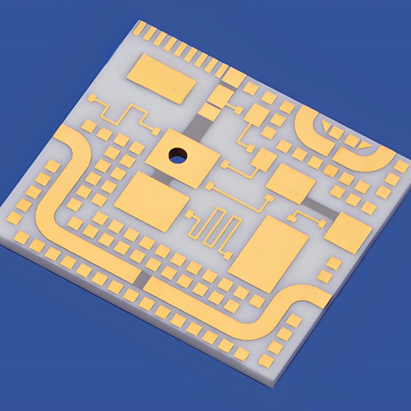
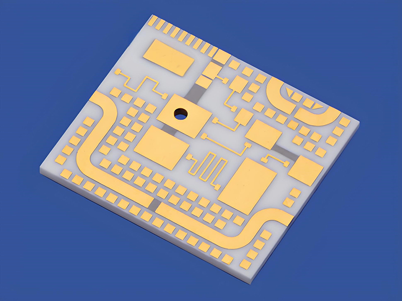
Ceramic Substrate Metallization
Customization Supported: Yes
Shipping Location: Shenzhen, Guangdong Province, China
Brand: Dinghongrun
E-mail: dhr@dinghongrun.com
WhatsApp: +8613629515219

Core Application Fields
1. Power Electronics (Dominant Market)
- IGBT/DBC Modules:
Copper-clad (120-300μm) alumina (Al₂O₃) or aluminum nitride (AlN) substrates support >1000A current with thermal conductivity >24W/(m·K). Key applications: EV power control and photovoltaic inverters. - IPM Modules:
Metallization enables multi-chip interconnects, sustaining >150°C junction temperatures (e.g., Mitsubishi 7th-gen IPM uses AlN + copper pillar arrays).
2. RF/Microwave (High-Frequency Applications)
- 5G Base Station GaN PAs:
Gold-plated (5-20μm) AlN substrates replace PCBs, reducing dielectric loss (tanδ <0.001) for 28/39GHz mmWave operation. - Phased Array Radar T/R Components:
Beryllium oxide (BeO) metallization dissipates high power density while matching GaAs chip CTE (6.5ppm/K).
3. Optoelectronics & Sensing (Precision Interconnects)
- Laser BAR Bonding:
Au-Sn eutectic bonding on ceramic carriers achieves <0.3K/W thermal resistance (e.g., TRUMPF 3kW semiconductor lasers). - MEMS Pressure Sensors:
Zirconia (ZrO₂) metallized sealing rings enable wafer-level hermeticity (<10⁻⁸ mbar·L/s leak rate).
4. Advanced Packaging (Emerging Frontier)
- Automotive LiDAR:
LTCC substrates with silver paste metallization integrate transceiver modules (CTE mismatch <2ppm/°C). - Quantum Computing Chips:
Superconducting circuits on metallized Al₂O₃ substrates (surface roughness <50nm) minimize microwave loss.
Technical Value Proposition
Metallized layers achieve >50N/mm Cu-ceramic bond strength* through microstructure control (e.g., Mo-Mn transition layers). Maintains electrical stability across -55°C to 850°C thermal cycling, providing foundational reliability for extreme-environment systems.