

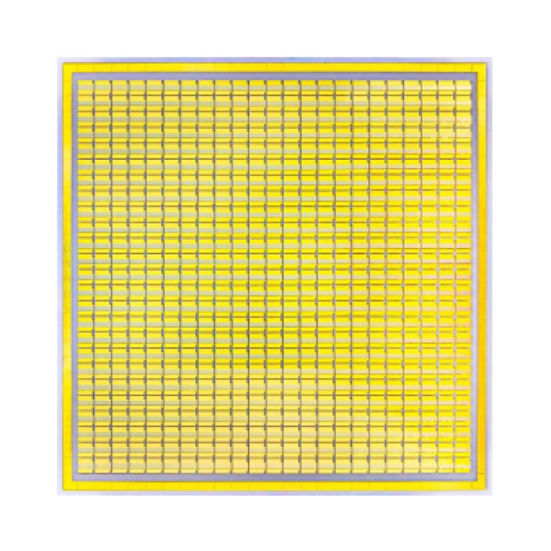
Semiconductor High-Power Laser Substrates
Customization Supported: Yes
Shipping Location: Shenzhen, Guangdong Province, China
Brand: Dinghongrun
E-mail: dhr@dinghongrun.com
WhatsApp: +8613629515219
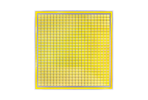

Core Functionality: Thermal Management & Structural Support
1. Thermal Conduction Hub
- Substrates (e.g., AlN/Al₂O₃ ceramic) bridge laser bars (>1kW/cm² heat flux) and heat sinks
- Metallization (Au/Cu) ensures thermal resistance <0.3K/W (e.g., <40℃ temperature rise in 3kW lasers)
- High thermal conductivity materials (AlN: 180W/m·K) prevent hotspots and maintain photoelectric efficiency
2. Mechanical Stress Coordination
- Au-Sn eutectic bonding matches CTE differentials:
▪ Laser chip CTE: ≈7ppm/K
▪ Ceramic CTE: ≈4.5ppm/K - Achieves >10⁷ thermal cycles without solder joint failure
3. Electrical Interconnection Platform
- Precision circuitry enables:
▪ Low-inductance parallel connection (<1nH)
▪ Nanosecond pulse current handling (>100A)
▪ EMI suppression
4. Sealed Packaging Foundation
- Hermetic sealing (<10⁻⁸ mbar·L/s leak rate) prevents moisture/oxygen corrosion
- Metallization bond strength >50N/mm (Mo-Mn method) ensures stability at -40℃~150℃
5. Optical Alignment Benchmark
- Micro-hole arrays/alignment marks with ±2μm precision
- Ensures beam collimation (divergence angle <10°)
Technical Essence: Resolves thermal-mechanical-electrical coupling failures in high-power-density systems through coordinated material-ceramic, structure-metallization, and process-brazing design. Enables >100,000-hour lifespan for kilowatt-level laser systems.