

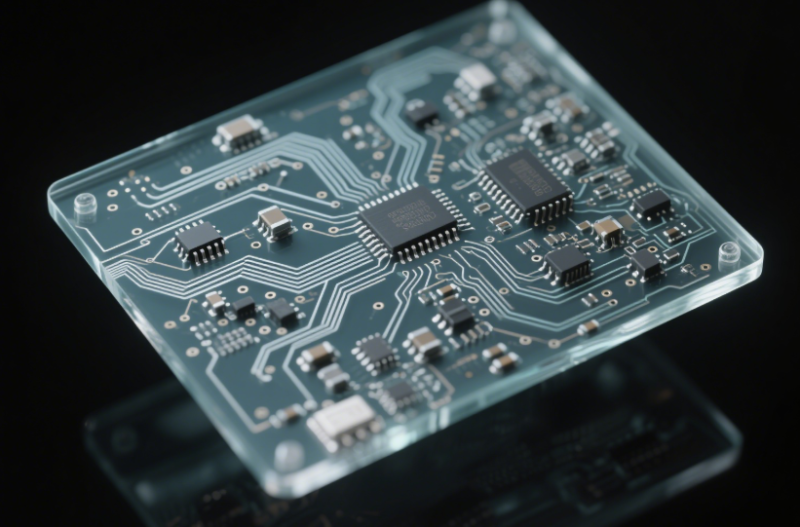
Glass via technology: innovator and limitation analysis of circuit board high-frequency performance
In the traditional high-speed circuit design, the signal integrity loss in the tiny hole is like an unsolved puzzle, which continues to puzzle engineers. The roughness, voids and uneven thickness in the copper plated through-hole are like invisible energy funnels. Once the high-frequency signal enters, it will be like a bullet. until Glass through hole With the advent of technology, this game changing technology began to reshape the performance boundary of circuit boards.
Signal revolution in high-frequency field
In the millimeter wave band and high-speed digital signal transmission, the glass vias act as a precise high-speed signal steward:
- The secret of low dielectric loss: Glass material has a very low dielectric loss factor (Df) in essence, which is a fraction of the standard epoxy resin. When the high-frequency current passes through, it generates much less heat, and the signal energy increases significantly. Imagine the existence of a lossless pipeline, and the high-frequency signal transmission is unimpeded.
- Smooth and even blessing: The hole wall generated by laser etching is as smooth and flat as a mirror, and then coated with a uniform thin copper layer, which fundamentally avoids signal reflection. Each hole is like a perfect channel to minimize the interference noise in the signal path, especially in the high-speed circuit design link of 40Gbps and above.
- Auxiliary function of glass substrate: The high-performance glass substrate itself has a very low dielectric constant (Dk), which reduces the parasitic capacitance of the conductor in high-speed transmission state. Especially when the through holes are densely arranged on the circuit board, the low Dk characteristic can alleviate the problem of cross talk between signals.
Stable physical support
The coefficient of thermal expansion (CTE) between glass material and copper conductor is almost the same as that of resin based material. Even in the face of reflow impact up to 200 ° C, glass vias can maintain structural stability and reduce the risk of solder joint cracking – this feature has become a rigid support in advanced packaging requiring multiple high-temperature treatments. On the other hand, the inherent hardness of the glass makes the ultra-thin substrate structure firm and not easy to warp during stacking and operation.
To be efficient in 3D space
When the density of circuit board becomes the bottleneck of design, the vertical direction is the new development space. Glass vias directly support circuit board thinning and multi-layer 3D stack integration, realizing the Z-axis interconnection revolution. The signal transmission path between vertical layers is extremely simplified, the signal delay is shortened, and the power consumption is also significantly reduced. This feature of high density and low latency just meets the core requirements of high-performance computing chips and advanced sensor modules.
Challenges remain
Of course, this revolutionary technology is not without limitations:
- Cost gate: Precision laser processing is extremely harsh to the process environment. The yield pressure and high equipment investment make its price far higher than that of traditional mechanical drilling and electroplating holes.
- Technical complexity: Core technologies such as precision control of glass substrate drilling and high-quality metallization are higher barriers for manufacturers, which are currently concentrated in a few enterprises with cutting-edge technology.
- Application circle: Not all circuit boards need to carry gigabit high-frequency signals or challenge micron level stacking. The use of glass vias for simple consumer electronic devices will not pay off.
Conclusion: A continuous high-frequency upgrade
Under the background that high frequency and high density have gradually become the standard configuration of high-performance electronic products, glass via technology is rewriting the new rules of circuit board performance. With the explosion of demand for millimeter wave communications, low orbit satellite networks, and artificial intelligence chip clusters, we see glass vias begin to expand to larger scale applications. Although this technology is currently limited to the high-end field, when the manufacturing process is gradually mature and the cost structure is optimized, its far-reaching impact in the high-performance electronics field will inevitably reshape the entire industry rule – those designs that once adhered to the traditional through-hole technology will gradually lose competitiveness in the high-frequency world. Future circuit boards will not wait in silence. They are completing self-expression in the signal world at a higher frequency through glass via technology.