

Photoetching Technology: the Core Technology of Modern Electronic Manufacturing
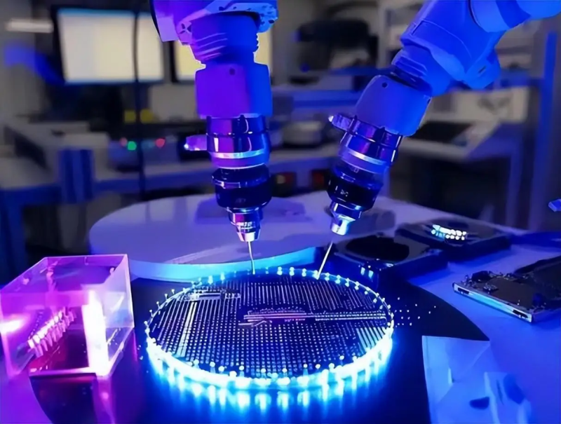
Photoetching is one of the key steps in modern semiconductor manufacturing, which is widely used in chip production, microelectronic device manufacturing and integrated circuit manufacturing. This technology accurately transfers the designed circuit pattern to the surface of silicon wafer or other materials through illumination, mask and chemical reaction, providing a basis for the production of high-performance electronic equipment. This paper will discuss the basic principle, development process and application in modern electronic industry of photolithography and etching technology.
1、 Basic principles of photolithography and etching technology
Photoetching and etching are often used together in electronic manufacturing. Lithography transfers the designed pattern to the photoresist through illumination, while etching uses chemical solution or physical means to remove unnecessary parts, thus retaining the circuit pattern.
- Photolithography process : First, a layer of photoresist is coated on the silicon wafer surface, and the designed pattern is projected onto the photoresist through the mask. After exposure, the photoresist undergoes chemical changes, and then retains the required pattern part through the development process.
- Etching process : Etching is performed after photolithography, and the uncovered part of photoresist is removed by chemical etching or plasma etching technology. Etching can be wet (chemical solution) or dry (plasma, reactive ion etching, etc.). Through etching technology, materials can be removed with high precision to form tiny circuit structures.
2、 Development history of photolithography and etching technology
Since the lithography technology came out in the late 1950s, it has experienced a long development process from simple exposure to complex multiple patterns. With the progress of semiconductor technology, photolithography technology continues to improve resolution and accuracy. With the promotion of Moore’s Law, chip manufacturers’ demand for higher resolution is increasing, which makes lithography technology develop to smaller nodes.
Etching technology has gradually improved with the complexity of integrated circuits, especially the emergence of dry etching technology, which makes it possible to transfer patterns on a smaller scale. Today, the etching process has been able to deal with nanoscale structures, realizing accurate replication of fine patterns in advanced manufacturing processes.
3、 Application of Photoetching Technology in Modern Electronic Industry
Photoetching technology is widely used in the modern electronic industry, and is the core technology for manufacturing chips, micro sensors, MEMS (Micro Electro Mechanical Systems) and other electronic devices.
- Semiconductor chip manufacturing With the continuous reduction of chip size, higher requirements are put forward for photolithography and etching technology. Advanced lithography technology enables the chip to accommodate more transistors, improving computing performance and efficiency. At the same time, the etching process must also maintain high precision to ensure the good connection and reliability of the chip circuit.
- Micro sensors and MEMS devices Photoetching and etching technology makes it possible to produce MEMS devices such as micro sensors, accelerometers, gyroscopes, etc. These micro devices are widely used in smart phones, automobiles, medical equipment and other fields.
- Integrated Circuits and Microelectronic Systems With the continuous progress of integrated circuit technology, photolithography and etching technology has become an important part of microelectronic system manufacturing. Miniaturization and high-density integrated circuit manufacturing depend on the synergy of photolithography and etching technology.
4、 Challenges and development direction of photolithography and etching technology
Although the lithography and etching technology has made significant progress, with the chip size entering the nanometer level, the traditional lithography and etching technology is facing some technical bottlenecks. The following are the future development directions:
- Extreme Ultraviolet (EUV) Lithography Technology EUV lithography, as a new generation of lithography technology, can provide a shorter wavelength light source and further improve the pattern resolution. With the continuous maturity of EUV equipment, it is expected to become the mainstream technology of chip manufacturing in the future.
- Multiple exposure technique In order to solve the resolution limitation of traditional lithography technology, multiple exposure technology has been proposed to create more precise circuit patterns through the superposition of multiple exposures and lithography patterns.
- New Etching Materials and Processes With the complexity of etching process, new etching materials and methods are gradually applied. For example, using more selective etching chemicals can further improve the accuracy of the etching process and reduce errors.
conclusion
Photoetching technology is undoubtedly the core pillar of modern electronic industry, supporting the rapid development of semiconductor, microelectronics and related industries. From the early basic lithography to today’s high-precision etching technology, the entire process chain is constantly optimized and innovated. In the future, with the continuous breakthrough of technology, photolithography and etching technology will promote the development of chip manufacturing towards higher precision, smaller size and higher integration, and promote the innovation and application of intelligent devices.