

Integrated application analysis of photolithography and etching
Photoetching and etching technology is the core technology in modern semiconductor manufacturing, especially in the production of integrated circuits (IC), which plays a crucial role. With the progress of technology, the integrated application of photolithography and etching technology has continuously promoted the development of chip manufacturing technology towards smaller size, higher performance and lower power consumption. In today’s semiconductor manufacturing, photolithography and etching technology are not only separate process steps, but also interdependent and closely coordinated process systems. This paper will discuss the basic principles of photolithography and etching, their integrated applications and their importance in the semiconductor industry.
Basic principles of photolithography and etching
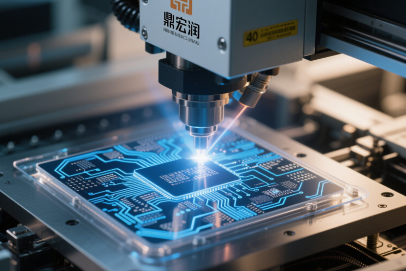
Photolithography The pattern on the mask is transferred to the substrate surface coated with photoresist by light irradiation. The specific step is to coat a layer of photoresist on the surface of the substrate, and then irradiate the ultraviolet light onto the photoresist through the mask through the photoresist. The photoresist will undergo chemical reaction according to the different light intensity. After developing, it will retain the desired pattern, and eventually form a micron or even nanometer structure.
Etching technology It is used after photolithography to remove some unprotected materials of photoresist by chemical or physical methods. Etching can be divided into wet etching and dry etching. Dry etching usually uses plasma or gas to react, which can accurately remove multi-layer materials and leave the desired pattern structure. Etching technology enables the pattern formed after photolithography to be further processed on the substrate, and finally made into the circuit structure required by the chip.
Integrated application of photolithography and etching
In semiconductor manufacturing, the combination of photolithography and etching technology enables high-precision manufacturing of micro – and even nano scale circuits. In a typical IC production process, photolithography and etching are often conducted alternately.
- Perfect combination of pattern transfer and precision machining
Lithography is used to transfer the circuit design pattern to the substrate surface, while etching is used to precisely remove unnecessary materials and finally leave the required circuit pattern on the silicon chip. This process is repeated several times to form the final chip structure. The integrated application of photolithography and etching enables semiconductor processes to achieve higher resolution and more accurate graphic details, and promotes the development of microelectronics technology.
- Multilayer metal interconnection and silicon wafer manufacturing
In modern integrated circuits, in addition to building tiny transistors, multi-layer metal interconnection is also required to realize the connection between different circuits. Lithography and etching play an important role in this process. Lithography is used to define the pattern of each layer of metal circuit, and etching is used to conduct deep processing on the metal film to ensure accurate connectivity between circuits. Through these processes, the signal transmission within the chip can maintain low delay and high efficiency.
- Improve process yield
With the continuous miniaturization of chip technology, the traditional lithography and etching technology is facing the precision challenge in very small size. In order to ensure yield, photolithography and etching processes need to be highly integrated and precisely matched. For example, in the advanced extreme ultraviolet (EUV) lithography technology, the process of lithography and etching is more closely combined. Through more fine pattern transfer and high-precision etching, chip manufacturing can meet the requirements of smaller size and higher integration.
- Application of new materials and new processes
With the development of semiconductor technology, more and more new materials are used in chip manufacturing, such as high k materials, copper, low k materials and so on. In the processing of these new materials, the integrated application of photolithography and etching technology is particularly important. Different materials have different etching difficulties, so targeted technical support is needed to ensure the accuracy and effect of each material. At the same time, with the emergence of 3D integrated circuit and advanced packaging technology, the integrated application of photolithography and etching is also developing towards more complex structures, promoting the diversification of semiconductor manufacturing processes.
Challenges Faced by Integrated Applications of Lithography and Etching
Although the integrated application of photolithography and etching technology has greatly promoted the development of the semiconductor industry, as chip manufacturing has entered the nanometer level, it still faces a series of challenges:
- Resolution limit : As the process nodes continue to shrink, the resolution of traditional lithography technology gradually approaches the physical limit, limiting the further reduction of chip size. In order to break through this bottleneck, extreme ultraviolet (EUV) lithography technology is becoming the key to future development.
- Etching precision : The precision of etching process directly affects the stability of chip performance. With the improvement of process precision requirements, etching technology needs to be constantly optimized to avoid over etching or non etching.
- Diversity of materials With the continuous introduction of new materials, how to adjust the photolithography and etching process to meet the processing needs of different materials has become a challenge that cannot be ignored.
summary
As a key link in semiconductor manufacturing, photolithography and etching technology has been widely used in the production of a variety of advanced chips. Through the precise combination of photolithography and etching technology, modern semiconductor technology can realize chip products with smaller size and higher performance. Despite the challenges of technology and materials, the integrated application of lithography and etching is still the core force to promote the development of the semiconductor industry. With the continuous progress of technology, we have reason to believe that this process system will continue to lead the direction of chip manufacturing in the future.