

Current Status and Future Development of Semiconductor Etching Technology
The development of semiconductor technology has profoundly changed the design and manufacturing of modern electronic equipment. As one of the core processes in semiconductor processing, etching technology plays a crucial role. With the continuous development of integrated circuit (IC) design, the requirements for precision and performance are increasing. Etching technology is also evolving to meet these requirements. This paper will discuss the basic principle, application status and future development direction of semiconductor etching technology.
1、 Basic Principles of Semiconductor Etching Technology
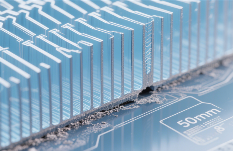
Semiconductor etching technology, in short, is the process of removing specific areas on the surface of semiconductor materials by chemical or physical methods. It is usually divided into wet etching and dry etching.
1. Wet etching
Wet etching usually uses chemical solutions to etch the surface of semiconductor materials. This method can accurately remove unnecessary materials by controlling the concentration, temperature and etching time of the solution. Wet etching is suitable for etching in large areas, with simple operation and low cost, but it has some limitations on precision and detail control.
2. Dry etching
Dry etching is achieved through physical and chemical processes such as ion bombardment and plasma reaction. This method can provide higher precision, especially in the nanometer scale, and can etch very detailed patterns. Dry etching is widely used in modern integrated circuit manufacturing process, especially in manufacturing high-density chips, which plays an irreplaceable role.
2、 Application of semiconductor etching technology
With the continuous development of integrated circuits to miniaturization, high-speed and multi-function, semiconductor etching technology has become increasingly important in many fields. The following are some main application directions:
1. Manufacturing of integrated circuit (IC)
Integrated circuit is the core component of electronic products, and its production process involves a large number of etching processes. In the process of chip manufacturing, etching technology is used for pattern transfer, metal layer stripping and fine processing of micro structures such as transistors. As the size of the chip continues to shrink, the precision of the etching process is required to be higher and higher. Especially in the nano level process, the application of dry etching technology is crucial.
2. MEMS
MEMS technology integrates mechanical and electronic systems on tiny silicon based materials, and the application of etching technology can not be ignored. Precision components such as micro sensors and actuators can be manufactured by precise etching. MEMS is widely used in medical devices, automotive sensors, and consumer electronics, and its core is the etching process.
3. Optoelectronic devices
With the rise of optoelectronic technology, semiconductor etching technology plays an increasingly important role in optical fiber communication, lasers, solar cells and other fields. Etching process can accurately manufacture micro optical structures and improve the performance and stability of optoelectronic devices.
3、 Challenges of semiconductor etching technology
Although etching technology has made significant progress, it still faces a series of challenges in terms of high precision and efficiency.
1. Improvement of precision and resolution
With the continuous development of integrated circuits to smaller size, etching technology is facing the improvement of precision and resolution requirements. Especially in the process of nano chip manufacturing, how to ensure the integrity and accuracy of fine patterns in the etching process has become a difficult problem to be solved.
2. Material selection and etching selectivity
In semiconductor manufacturing, selective etching of different materials is an important challenge. For example, in the chip manufacturing process of multi-layer materials, different materials need to be selectively etched to prevent damage to other layers of materials. This requires the etching process to reach a higher level in chemical reaction, energy control and solution formulation.
3. Environmental friendliness
With the increasingly strict environmental protection regulations, chemicals used in traditional wet etching technology may cause some pollution to the environment. Therefore, how to develop more environmentally friendly and less toxic etching methods has become an important topic in the development of the industry.
4、 Future development direction
In order to meet these challenges, semiconductor etching technology is constantly innovating. The following are some directions for future development:
1. Nanoscale etching technology
With the progress of technology, nanoscale etching becomes possible, and the future etching technology will operate with high precision on a smaller scale. By combining advanced lithography technology, etching technology will make breakthroughs in higher precision and detail control, providing support for ultra high integration integrated circuits and electronic equipment.
2. Plasma etching technology
Plasma etching technology has become one of the mainstream technologies in high-end chip manufacturing due to its more accurate control capability and strong material adaptability. In the future, plasma etching technology will continue to be optimized to provide higher processing accuracy and lower production costs.
3. Environmental protection and low-cost etching technology
With the continuous improvement of environmental requirements, how to develop more environmentally friendly etching methods has become an important research direction. The use of green chemical and non-toxic chemical solutions will be the trend of future etching technology development, reducing the burden on the environment and the production cost.
5、 Conclusion
As an indispensable part of integrated circuit manufacturing, semiconductor etching technology is constantly innovating in the technological progress. With the improvement of precision, efficiency, environmental protection and other requirements, etching technology will continue to overcome challenges and meet new opportunities. The future semiconductor etching technology will be more precise and efficient, and will be widely used in more fields, promoting the further development of electronic technology.