

Glass Etching: Surface Engineering Revolution from Light Control to Chip Interconnection
The molecular layer on the surface of glass is quietly changing the face of modern industry. When the hydrofluoric acid solution reacts with silica, or the picosecond laser beam accurately bombards the glass surface, the etching process of the micro world is reshaping the physical properties of the glass—— This surface modification technology transforms glass from a transparent package to a functional carrier , opening up new possibilities in the fields of architecture, electronics, optics and medicine. From the brand logo of Huawei mobile phone cover plate to the glass through hole in 5G chip package, the etching process has become the core technology of precision manufacturing.
1、 How to reconstruct glass surface by etching
1. Accurate control of optical performance
The most direct change of etching to glass is light control. The micron scale concave convex structure (0.75-15 μ m depth) is made on the surface by chemical or physical methods, and the light occurs in the etching area Diffuse reflection effect To achieve a gradient effect from semi transparent to full fog face. In the automotive field, the uniform fog surface formed by sand blasting method can insulate the external view of the window while ensuring the daylighting; Laser etching can precisely control the light transmittance of specific areas on the medical microfluidic chip, and realize the visual monitoring of biological reaction process.
2. Enhancement and upgrading of interface performance
The rough surface after etching significantly improves the adhesion of glass. In microelectronic packaging, the surface roughness of laser induced etched glass substrate was controlled within 150 nm, which improved the peel strength of copper metal layer to 347.8 mN, much higher than the performance of untreated substrate. The principle is: Micro textured surfaces add mechanical bite points At the same time, the silicon hydroxyl exposed by chemical etching enhanced the bonding ability with metal atoms. This interface strengthening effect directly extends the wear-resistant life of the logo logo on the phone cover, and also ensures the long-term reliability of the copper through-hole in the chip package.
3. Micro construction of functional structure
In high-end applications, etching has gone beyond surface treatment to become a processing method for three-dimensional structures:
- Through hole interconnection : Picosecond laser makes a through hole with a depth width ratio of 20:1 on 100 μ m thick borosilicate glass, and the smoothness of the inner wall of the hole is less than 0.5 μ m, providing a low loss signal channel for chip packaging
- Microchannel network : Hydrofluoric acid gradient etching forms 10 μ m wide capillary channel on the medical diagnosis chip, with an accuracy of ± 0.8 μ m
- Optical microstructure : Ion beam etching produces anti reflection micro pyramid array on the lens surface, which increases the light transmittance to 99.6%
2、 Process selection and engineering adaptation
1. Chemical etching: a mature scheme for low-cost batch production
Hydrofluoric acid (HF) is still the mainstream etchant, and controllable corrosion is achieved by reacting with SiO ₂ (SiO ₂+6HF → H ₂ SiF ₆+2H ₂ O). The ammonium fluoride based etching solution popularized after 2023 will reduce the volatile toxicity by 40%, and the etching speed will reach 1.2 μ m/min. A single production line can process 200 pieces of glass of 300mm × 400mm specification per hour. However, the process faces two major limitations: when the depth width ratio is greater than 5:1, the side wall steepness is out of control, and the strong acid environment has high corrosivity to the equipment. At present, it is still irreplaceable in architectural decoration glass and household appliance panel.
2. Laser etching: the core breakthrough of high-precision scenes
Picosecond laser technology (pulse width 10 ⁻⁻ ² s) has brought about a “cold processing” revolution:
- The heat affected zone approaches zero To avoid microcracks caused by traditional processing
- Energy density up to 10 ¹ ≮ W/cm ² , achieving nanometer etching precision
- Computer path programming Support direct writing of complex 3D structures
The laser induced etching (LIDE) technology jointly developed by Germany Tongkuai Group and SCHMID, through the synergy of laser modified areas and wet etching, improves the TGV processing efficiency to 290 holes/second, and reduces the processing time by 90%. This technology has become the first choice for 5G RF module packaging and microfluidic chip manufacturing.
3. Engineering adaptation of mixing process
Leading edge applications are breaking through the limitations of single process:
- Photolithography composite process : Photoresist mask+HF etching optical glass The diffraction grating is fabricated on the, and the line width accuracy is ± 0.1 μ m
- Plasma assisted etching : Fluoride gas plasma etching quartz glass to achieve millimeter wave waveguide structure with aspect ratio of 10:1
- Sand blasting+laser combination : The architectural glass is first sandblasted to form a basic fog surface, and then laser carved light transmission patterns, giving consideration to efficiency and artistry
3、 Industrial application and value reconstruction
1. Electronics industry: double innovation from appearance to core
- Surface decoration layer : Huawei P20 mobile phone rear cover adopts HF etching logo, and the abrasion resistance of the etching area with a depth of 15 μ m is increased by three times
- Functional carrier layer : Laser etches transparent conductive grid on the vehicle mounted instrument panel glass, and the resistance uniformity reaches ± 1.5%
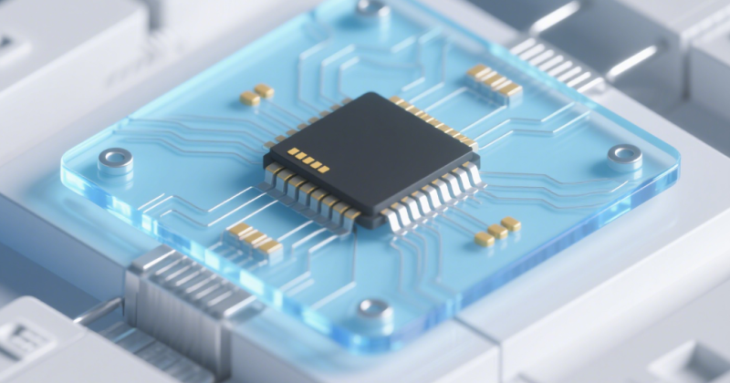
- Chip packaging substrate : TGV technology reduces the cost of glass interlayer to 1/8 of silicon base, and the insertion loss is only 0.069dB/mm (60GHz)
2. Optics and medicine: breakthrough in performance boundary
- Optics : Femtosecond laser etched the anti reflection microstructure on the lens surface, reducing the reflectivity of 400-700nm band to 0.1%
- Implantable equipment : Borosilicate glass is plasma etched to form microporous structure, realizing zero corrosion in body fluid environment for 10 years in cardiac pacemaker
- Diagnostic chip : The microfluidic chip made by wet etching realizes single cell capture analysis through a 30 μ m deep reaction chamber
3. Building and energy: value optimization of large-scale manufacturing
- Energy saving curtain wall : Gradient etched glass curtain wall (with light transmittance of 30% – 70% distributed in regions) reduces building cooling energy consumption by 40%
- PV module : Hydrofluoric acid etched solar panel glass, and the surface texture improved the photoelectric conversion efficiency by 1.2%
- Decorative components : The etching process without protective layer reduces the production cost of art glass by 35%, and improves the pattern accuracy to 0.5mm line width
4、 Technological evolution and future challenges
1. Rebalance of precision and efficiency
Existing processes face double challenges: chemical etching has low cost but limited accuracy (minimum feature size>50 μ m); Although laser etching reaches micron level precision, the equipment investment is over one million dollars. Emerging solutions include:
- Mixed etching system : LIDE technology developed by Tongkuai Group integrates laser and wet unit, reducing the processing cost of TGV to $150/piece
- Multi beam parallel processing : Space light modulator beam splitting technology achieves 32 channels of synchronous etching, and the throughput is increased by 5 times
2. Breakthrough in environmental protection
Although the ammonium fluoride based etching solution reduces the volatility of hydrofluoric acid, the waste liquid treatment still accounts for 25% of the production cost. Focus on frontier exploration:
- Closed loop regeneration system : Shanghai Cirou Co., Ltd. has developed an electrolytic regeneration device for etching solution, with a reagent recovery rate of 82%
- Supercritical CO ₂ etching : Laboratory stage technology, using supercritical fluid to carry reagent to achieve zero wastewater discharge
3. Interdisciplinary integration and innovation
- Optoelectronic device integration : Laser etched optical waveguide+copper via interconnection in glass substrate, providing optoelectronic co packaging solution for silicon optical chips
- Smart response surface : Thermal material coating+selective etching, developing “dynamic glass” with adjustable light transmittance
- Bioactive interface : Microporous etched glass loaded with stem cell growth factor for surface functionalization of orthopedic implants
Conclusion: Deep value of surface engineering
Glass etching The essence of the evolution history of technology is The Cognitive Transition from “Removing Materials” to “Constructing Functions” 。 When picosecond laser carves capillary network on microfluidic chip, and when ammonium fluoride etching solution weaves light trapping structure on the surface of photovoltaic glass, the industry is witnessing the transformation of surface engineering from auxiliary process to core manufacturing link.
With the continuous downward exploration of the cost of laser induced etching, the maturity of environmental protection technology and the explosion of interdisciplinary applications, etched glass has jumped from the aesthetic carrier of architectural decoration to the core functional material of high-frequency communication, precision medical treatment and clean energy. In the future, when every piece of glass can become a circuit board, optical element or bioreactor, we will redefine the value of “transparency” – it is not only the channel of light, but also the carrier of information, energy and life.
Essence of Etching : Create opacity in transparency, build roughness in smoothness, and design heterogeneity in homogeneity – this precise manipulation of the material surface is the engineering art of human beings to transform intangible ideas into physical functions.