

Glass via interconnection technology: packaging revolution of high-frequency chips
In the field of high-end chip packaging, a silent technological change is taking place. When the high frequency loss and complex process of silicon substrate gradually become the bottleneck of computing power improvement, a new interconnection technology—— Glass through hole (TGV) is showing amazing potential in semiconductor laboratories and advanced production lines. Different from traditional silicon through-hole (TSV), TGV passes High quality borosilicate glass or quartz glass as intermediate layer And forming a vertical conductive channel on the substrate to realize three-dimensional interconnection between chips. This technology transformation not only solves the problem of high-frequency signal loss, but also reduces the packaging cost to One eighth 。
1、 Technical core: precision engineering from through-hole to interconnection
1. Pore forming technology: technological breakthrough of micron precision
The manufacturing of glass through holes shall meet High aspect ratio, narrow pitch and low roughness The mainstream process shows diversified development:
- Laser induced etching (LIDE) : By selectively changing the molecular structure of glass with picosecond laser, and then etching with hydrofluoric acid solution, a through hole with a depth to width ratio of 20:1 can be formed at a rate of up to 290 holes/s And the side wall is smooth without cracks, becoming the most feasible scheme for mass production at present.
- Plasma etching : Perfluorocyclobutane/argon plasma is used to etch quartz glass, the side wall roughness can be controlled below 150 nm, but the etching rate is less than 1 μ m/min, and aluminum mask and photolithography process are required, so the cost is high.
- Limitations of other processes : Sand blasting method (aperture>200 μ m), focusing discharge method (poor hole perpendicularity) and photosensitive glass method (structural deviation due to high temperature treatment) have gradually withdrawn from the advanced packaging field due to precision or cost problems.
2. Metallization: balance between adhesive force and electrical property
The glass surface is smooth and chemically inert, and poor adhesion to copper is the core challenge:
- Seed layer innovation : The 50 nm TiW layer by magnetron sputtering can increase the glass metal peel strength to 347.8 mN, which is better than the 244.1 mN of the silicon based titanium tungstate scheme.
- Adhesive reinforcement layer : Metal oxide adhesive aids (such as 5~20 nm thick oxide layer) can break through the peel strength through mechanical anchoring and chemical bonding 6 N/cm It overcomes the difference of thermal expansion coefficient between copper and glass (17 × 10 ⁻⁶⁶/° C vs 3 × 10 ⁻⁶⁶/° C).
- Fill Scheme Selection : The solid hole electroplating (copper filling) ensures high-frequency conductivity, while the thin layer electroplating (copper plating on the inner wall of the hole) reduces the cost by 30% while meeting the 60 GHz signal transmission.
3. Through hole structure design: bottom logic of electrical performance
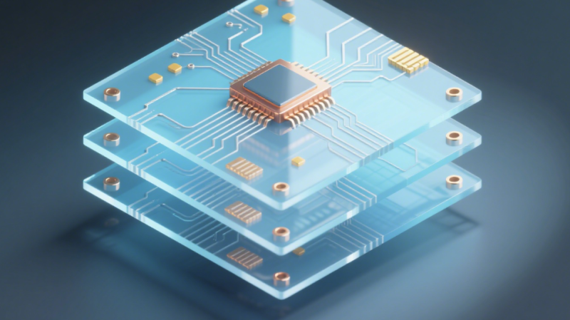
- Vertical interconnection architecture : TGV is essentially through Glass substrate Internal Metallized via to realize vertical conductive channel between chips , replacing the traditional horizontal wiring, greatly reducing the signal transmission distance.
- Re routing Layer (RDL) integration : After the through hole metallization is completed, it is necessary to build high-density copper wiring on the front and back of the glass substrate, and form a micron level circuit through the half addition method (SAP). The line width can be controlled within 2 μ m.
2、 Performance advantage: subversive value of high-frequency scenarios
1. High frequency loss reduction: the core guarantee of 5G millimeter wave
- Breakthrough in dielectric properties : The dielectric constant of glass (ε ≈ 5.5) is only that of silicon substrate (ε ≈ 11.7) One third The loss factor is 2~3 orders of magnitude lower, which reduces the signal insertion loss in the 5G millimeter wave band (24~40 GHz) to 0.55 dB/mm.
- Application case : The five layer glass stacked packaging antenna developed by Xiamen University realizes 77 GHz frequency band signal transmission through TGV, with insertion loss of only 0.31 dB (low frequency band) and 0.70 dB (high frequency band), and attenuation depth of 28 dB.
2. Cost and integration reconstruction
- Process simplification : The insulating property of the glass itself eliminates the deposition steps of SiO ₂ insulating layer necessary for TSV, reduces four core processes, and increases the yield by 15%.
- High density integration : TGV supports interconnection with aperture ≤ 10 μ m and pitch ≤ 20 μ m, improving the interconnection density between HBM (high bandwidth memory) and CPU 10X , bandwidth increased by 6 times.
3. Reliability improvement: thermal and mechanical stability
- Thermal expansion matching : The thermal expansion coefficient of borosilicate glass (3.3 × 10 ⁻⁶⁶/° C) is close to that of silicon chip (2.6 × 10 ⁻⁶⁶/° C), reducing the risk of solder joint failure caused by thermal cycle.
- Mechanical resistance : The warpage of glass substrate with thickness of 100 μ m is less than 5 μ m, while that of silicon substrate with the same thickness is more than 20 μ m.
3、 Application scenario: from RF medical treatment to computing chip
1. 5G RF front-end
- Antenna integration : The glass substrate integrated waveguide (SIW) is combined with TGV to realize 60 GHz conductor back coplanar waveguide, with insertion loss of only 0.069 dB/mm and size reduction of 56%.
- Filter miniaturization : TGV 3D inductance Q factor reaches 55 (6 GHz frequency band), combined with MIM capacitor, the size of the band-pass filter is reduced to 1.04 λ g × 0.27 λ g, and the bandwidth fraction exceeds 31%.
2. Medical electronics
In implantable devices such as cardiac pacemakers, TGV provides Air tight packaging and biological compatibility Keep the electrical stability for more than 10 years under the corrosive environment of body fluid.
3. High performance computing
- Intel Data Center Solution : The glass intermediate layer realizes 2.5D integration of CPU and HBM, reducing latency by 40% and power consumption by 50%.
- Alternative FC-BGA base plate : The glass substrate increases the carrying capacity of bare chips by 50% and reduces the thickness by 50%, helping AI chips break through the 15 kW power consumption wall.
4、 Challenge and evolution: the key path of industrialization
1. Mass production bottlenecks and solutions
- Brittleness control : Ultra thin glass (<50 μ m) is strengthened by polymer lamination, and its bending strength is increased by 300%.
- Thermal optimization : Insert aluminum nitride cooling column in TGV, and increase the thermal conductivity from 1.4 W/mK to 180 W/mK 。
2. Cost reduction path
- Equipment localization : The localization of laser induction equipment has reduced the manufacturing cost of TGV from 500/piece to 150/piece.
- Panel level process : 1 m × 1 m large size glass substrate is adopted, and the number of chips processed at a single time is increased by 20 times.
3. Technology convergence trend
- Optoelectronic device integration : Utilizing the transparency of glass, microlens array is integrated in the TGV substrate to achieve low loss coupling of optical communication wavelength.
- 3D Stacking Breakthrough : Multilayer glass wafer stacking combined with micro bump technology reduces the interconnection distance between chips to 10 μ m.
Conclusion: Industrial value of glass based interconnection
The essence of glass via interconnection technology is Through the coordination of insulating substrate and vertical interconnection, the electrical signal transmission path is reconstructed in high-frequency and high-density scenes 。 From the five layer stacked antenna of Xiamen University to the glass intermediate layer data center chip of Intel, TGV is opening a new track in the field of high-frequency communication and high-performance computing.
With the decrease of laser induced etching cost and the maturity of adhesion enhancement process, TGV is expected to realize the transformation from “Technical substitution” to “architecture definition” Span. When the glass substrate becomes the core carrier of 3D integration, chip packaging will move from “silicon binding” to “freedom of light”, opening the dual ceiling of physical space and electrical performance for 6G terahertz communication, silicon optical integration, and memory computing integration.
Dialectics of technology : The rise of TGV is not a simple replacement for TSV, but opens up a new battlefield in high-frequency and low-cost dimensions – just like the long-term coexistence of optical fiber and copper cable Glass and silicon will form a binary system with complementary functions in the computing revolution 。
Attached table: Comparison of mainstream TGV pore forming processes
| Process method | Minimum aperture (μ m) | Aspect ratio | Side wall roughness | Mass production potential | Applicable scenarios |
|---|---|---|---|---|---|
| Laser induced etching | ten | 20:1 | <0.5μm | ★★★★☆ | High frequency chip, micro sensor |
| Plasma etching | twenty | 10:1 | <150nm | ★★★☆☆ | High precision RF module |
| Photosensitive glass method | fifteen | 15:1 | <1μm | ★★☆☆☆ | Special structure device |
| Focusing discharge method | twenty | 8:1 | Uneven | ★★☆☆☆ | Large aperture general purpose device |
| Sandblasting | two hundred | 5:1 | >5μm | ★☆☆☆☆ | Obsolete, basically no longer used |