

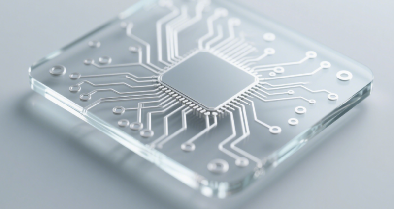
Laser etching: unlock the core key for high-precision manufacturing of TGV glass vias
In the wave of semiconductor packaging technology evolving to 3D integration, Glass through hole ( TGV )With the high frequency electrical characteristics, excellent insulation and adjustable coefficient of thermal expansion of glass materials, technology is becoming a critical path to break through the bottleneck of traditional silicon via (TSV) technology. To achieve high-precision, high-efficiency, and low damage glass through hole manufacturing, laser etching technology, with its non-contact processing, strong three-dimensional structure adaptability, and controllable heat affected zone, has become the core process support to promote TGV technology from laboratory to mass production.
1、 TGV technical bottleneck and engineering value of laser etching
As a vertical interconnection structure, glass vias shall meet Height depth width ratio (above 10:1), smooth hole wall without cracks, and controllable through hole diameter (10-100 μ m) And other strict requirements. There are obvious shortcomings in traditional mechanical drilling, sand blasting or wet etching:
- Sandblasting : Low machining precision, easy to produce microcracks and edge collapse at the hole edge, difficult to meet the requirements of high-density interconnection
- Wet etching : The isotropic characteristics lead to poor perpendicularity of the side wall, and the depth width ratio is usually difficult to break through the limit of 1:1
- Dry plasma etching : Complex process and low efficiency, difficult to adapt to large-scale mass production requirements
Laser etching technology can achieve precise removal or modification of glass through the interaction of high-energy photons and materials, and fundamentally overcome the above limitations. Its core values are as follows:
- Machining precision leap : Femtosecond/picosecond laser can realize<10 μ m aperture processing, and the position accuracy reaches micron level
- Minimal heat affected zone : Ultra short pulse (<10ps) realizes “cold working” to avoid micro cracks caused by thermal stress
- Strong adaptability of three-dimensional structure : It can handle complex hole types (blind holes, through holes, tapered holes) and structures with high aspect ratio (up to 100:1)
- High process flexibility : The hole wall roughness (Ra ≤ 0.08 μ m) and cone angle (0.1 ° – 30 °) can be controlled by parameter adjustment
2、 Classification and physical mechanism of laser etching technology
According to the interaction principle of laser and glass, the mainstream laser technology in TGV manufacturing can be divided into two categories:
(1) Direct laser ablation
- Principle : High energy density lasers (such as CO ₂ laser, UV nanosecond laser) directly vaporize glass materials to form through holes
- Applicable scenarios : Glass substrate with low requirements for aperture consistency and thin thickness (<200 μ m)
- Technical pain points :
- Heat accumulation leads to obvious heat affected zone (HAZ), and recast layer and microcrack are easily generated around the hole
- High roughness of hole wall (Ra>1 μ m), requiring secondary polishing
- Taper control is difficult, and the depth width ratio is usually limited to below 5:1
(2) Laser Induced Deep Etching (LIDE)
- Physical mechanism : Using ultra fast laser (femtosecond/picosecond) to induce non thermal phase transformation of glass, the etching rate of the modified area is increased 100 times
- Step 1: Laser modification : Picosecond/femtosecond laser focuses on the interior of the glass, and causes nonlinear ionization through multiphoton absorption, which leads to the disorder of the glass network structure (amorphous)
- Step 2: selective etching : When the modified glass is immersed in hydrofluoric acid (HF) solution, the etching rate of the modified area is significantly higher than that of the unmodified area (up to 300 times)
- Technical advantages :
- Realize true “no thermal damage” processing, and there is no microcrack on the edge
- The depth width ratio breaks through 10:1 (up to 100:1), and the side wall smoothness reaches optical grade
- Support one-time forming of complex three-dimensional structures (such as hourglass shaped and V-shaped holes)
Case : Germany LPKF’s Vitrion system uses picosecond laser (pulse width<3ps) and HF etching to achieve through hole processing with a depth width ratio of 50:1 and an aperture of 20-100 μ m, with a hole forming rate of 290 holes/s and a hole roundness error of<3 μ m.
3、 Key process chain and parameter control of laser induced etching
To achieve high-quality TGV, it is necessary to precisely control the synergy between laser parameters and chemical etching:
- Laser energy control window :
- Too low energy: the modification depth is insufficient, and the etching selection ratio decreases
- Too high energy: lead to glass carbonization, and the etching rate decreases
- Optimization point: picosecond laser single pulse energy is usually controlled at 10-50 μ J, and scanning speed is 200-1000mm/s
- Spatial positioning accuracy :
- The beam positioning error should be<1 μ m (using high-precision galvanometer and displacement platform)
- Dynamic compensation of focus position (to solve the aberration caused by the change of glass thickness)
- Etching dynamics control :
- HF concentration (5% – 20%): the higher the concentration, the faster the etching rate, but the side wall roughness increases
- Temperature control (25 ± 0.5 ℃): temperature fluctuation of 1 ℃ causes the etching rate to change by 7%
- Solution flow design: eliminate bubble attachment and ensure etching uniformity
- Defect suppression technology :
- Step etching strategy: multiple etching+intermediate cleaning to avoid accumulation of reaction by-products
- Ultrasonic assisted cleaning: remove the residual etching products in the hole
4、 Project application scenarios and value realization
High frequency RF device packaging
- 5G/6G millimeter wave antenna package (AiP) : Dielectric loss of glass substrate (Df= 0.0006@3GHz )It is only 1/30 of FR4. Combined with the laser etched precision TGV structure, the 60GHz band signal insertion loss is reduced to 0.2dB/mm
- Instance : The University of Florida has integrated a disc monopole antenna on a glass substrate, with a 62GHz radiation efficiency of 94%, a gain of 3.2dBi, and TGV for vertical transmission of millimeter wave signals between chips
2.5D/3D advanced packaging
- Glass adapter plate replaces silicon interlayer : Laser etching of TGV avoids the complex process of depositing insulating layer on silicon based TSV, and reduces the cost by more than 50%
- Intel glass substrate technology : In 2023, the glass substrate with a through-hole pitch of 75 μ m will be launched, which will increase the number of chips contained in a single package by 50%. It is planned to mass produce in 2026
MEMS/sensor hermetically sealed package
- Wafer level sealed package : HermeS of Schott ® The technology uses laser etching TGV to achieve a fully sealed structure. The package volume is 80% smaller than the ceramic package, and the leakage rate is less than 5 × 10 ⁻⁻⁸ mbar · L/s
- Biosensor Applications : Transparent TGV supports optical detection channel integration, such as in situ fluorescence detection in microfluidic chips
5、 Technical challenges and innovation paths
thin Glass processing reliability
- Question : When the thickness is<100 μ m, the risk of fragmentation caused by laser processing stress
- Solution :
- Temporary bonding carrier technology (such as temporary bonding glue of HD Microsystems)
- Optimization of laser parameters: reduce single pulse energy and increase repetition rate
Metalized reliability bottleneck
- Insufficient glass metal bonding force : Difference of thermal expansion coefficient between copper and glass (copper 17ppm/K vs glass 3.8ppm/K) leads to interface delamination after thermal cycle
- Innovative process :
- Transition layer design: sputtered TaN/Ti/Cu composite layer (Ti layer enhances adhesion, TaN blocks diffusion)
- Low temperature atomic layer deposition (ALD): deposit 20nm alumina transition layer on the hole wall
Key points of cost control
- Efficiency improvement of laser equipment : Huari Laser Femto-1000 achieves a processing rate of 5000 holes per second
- Etching solution recycling : HF online concentration monitoring and automatic fluid infusion system (such as RENA’s intelligent etching line)
- Panel Level Processing : Expand the processing size from 300mm wafer to 510 × 515mm panel, and increase the material utilization by 40%
6、 Frontier development trend
- Hybrid laser technology : Picosecond laser modification+CO ₂ laser annealing, synchronously improving processing efficiency and surface quality
- Multiphoton polymerization assisted processing : Femtosecond laser induced two-photon polymerization generates 3D mask to realize submicron TGV structure
- Dry etching replaces HF : Develop dry etching process based on SF ₆/O ₂ plasma to solve HF environmental protection problems
- Digital twin process control : Dynamic correction of laser parameters through real-time monitoring of plasma spectrum (such as LIBS technology)
Conclusion: The value transition from precision machining to system integration
The application of laser etching in TGV manufacturing has gone beyond the role of a simple punching tool to become a core enabling technology that connects material properties and system functions. With the reduction of femtosecond laser cost, the improvement of intelligent process control, and the innovation of glass materials (such as Corning low melting point glass, AGC adjustable CTE glass), laser etching is promoting the evolution of TGV technology to higher density (via pitch<50 μ m), better high-frequency characteristics (above 110GHz), and stronger system integration capability (co packaging of optoelectronic devices). In cutting-edge fields such as AI computing chip, terahertz communication, quantum sensing, etc., TGV technology based on laser etching will become a key enabler to break through the physical limits of traditional packaging, and redefine the integration boundary and performance ceiling of electronic systems.