

Photoetching: the art of precise “carving” inside the chip
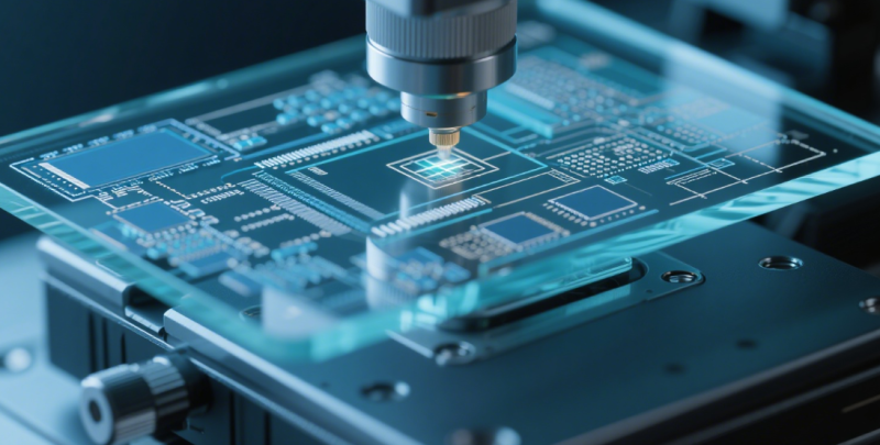
The core of modern science and technology is really inseparable from that small chip. The most delicate and critical steps in chip manufacturing are probably photolithography and etching Has. These two technologies are like a pair of tacit sculptors. They can accurately shape the circuit structure of the chip on the micro and even nano scale. Without them, today’s mobile phones, computers, and AI computing power cannot be talked about at all.
Lithography: draw a fine blueprint
Lithography is simply “carving with light”. It is responsible for transferring the designed circuit pattern to the silicon chip, just like an architect drawing a detailed construction blueprint.
The photolithography process is complex and precise. The wafer must first pass through Diluted hydrofluoric acid (DHF) treatment To remove the surface oxide layer and enhance the adhesion of photoresist. Then apply photoresist (a photosensitive material). Photoresist can be divided into positive photoresist and negative photoresist: positive photoresist becomes soluble after exposure, while negative photoresist becomes insoluble after exposure.
After gluing, the silicon wafer shall be Prebake To promote solvent volatilization and cure photoresist. Followed by Exposure The light shines on the photoresist through the mask to cause chemical reaction. Exposed Post bake It can reduce the standing wave effect and optimize the chemical structure inside the photoresist. Development The photoresist of a specific part is dissolved to make the pattern appear. After Dura mater (High temperature treatment) can further enhance the adhesion, corrosion resistance and protection of photoresist.
Etching: turning blueprints into reality
Lithography is just a temporary pattern formed on the photoresist, and the real “carving” work depends on etching. The purpose of etching is to selectively remove the material not protected by the photoresist, and accurately transfer the pattern on the photoresist to the material layer on the silicon wafer surface.
Etching is mainly divided into Wet etching And Dry etching 。 Wet etching uses chemical solutions to conduct isotropic etching, which has the advantages of good control and low cost. However, in a more refined process, it is easy to drill and erode, leading to a decline in precision. Dry etching, especially Reactive Ion Etching (RIE) Anisotropic etching with plasma is a mainstream technology of modern high-precision chip manufacturing, which has high precision and can carve vertical sidewalls.
Complement each other and challenge the limit
Lithography and etching in chip manufacturing Highly coordinated and cyclic 。 A complete set of chip circuits needs to go through dozens of such lithography etching cycles, stacked layer by layer, and step by step accurately.
As the chip manufacturing process continues to shrink to 3nm, 2nm or even smaller, lithography and etching technology is also facing Huge challenges : Problems such as optical diffraction limit, etching precision control, new material adaptation, and soaring cost need to be solved urgently. For example, the introduction of extreme ultraviolet (EUV) lithography technology puts forward new and higher requirements for the etching process.
In short Photolithography and etching are indispensable core links in chip manufacturing. They work together subtly to build the cornerstone of the modern digital world. Although these technologies are far away from ordinary people, it is these constant exploration and breakthroughs in the micro world that support our powerful computing power and convenient intelligent life today. Every time the mobile phone runs smoothly and every time the data is processed at a high speed, this pair of “precision sculptors” are behind the credit.