

Semiconductor etching technology: precision processing promotes the progress of microelectronics industry
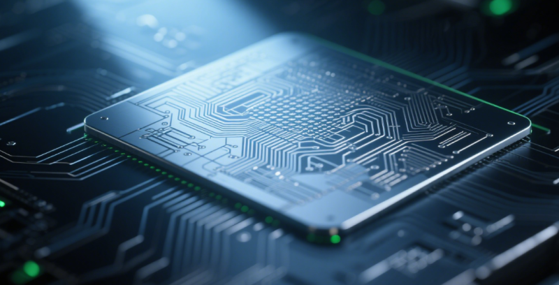
As one of the core processes in microelectronics manufacturing, semiconductor etching technology is widely used in integrated circuit (IC), micro electromechanical system (MEMS) and other fields. With the continuous development of the semiconductor industry, etching technology plays an increasingly important role in improving chip performance, reducing costs and promoting technological innovation. This paper will discuss the principle, application and future development trend of semiconductor etching technology.
Overview of semiconductor etching technology
Etching technology is a process that uses chemical, physical or laser methods to remove specific areas on the surface of materials. Semiconductor etching is usually used to form micro – or even nano scale fine structures on the surface of semiconductor materials such as silicon chips. In the production process of integrated circuits, etching technology can depict the details of the circuit through accurate pattern transfer, and then affect the performance and stability of semiconductor devices.
Application of semiconductor etching technology
- Integrated circuit manufacturing
Etching is one of the key steps in the production of integrated circuits. Through etching technology, complex circuit patterns can be carved on the surface of silicon chips to realize the functions and structures of chips. With the continuous improvement of chip integration, the precision requirements of etching technology are also increasing, which promotes the development and application of high-precision etching equipment.
- MEMS
Micro electro mechanical system (MEMS) is a high-tech field combining microelectronic technology and mechanical technology. Its applications cover a variety of products such as sensors, actuators, etc. The manufacturing process of MEMS requires precise etching at the micro or nano scale, so etching technology plays a crucial role in the production of MEMS. For example, the core components of air pressure sensors, accelerometers and other equipment are inseparable from the accurate etching process.
- Combination in photolithography
In photolithography, etching is used in the next step of pattern transfer. The lithography technology first transfers the pattern to the photoresist layer through light irradiation, while the etching technology is used to remove the unexposed part of the material, so as to achieve the final circuit pattern. Therefore, the perfect combination of photolithography and etching process is the key to the success of integrated circuit manufacturing.
- Promotion of nanotechnology
With the continuous development of nanotechnology, the application range of etching technology is also expanding. Etching operation on nanometer scale requires higher precision and control ability. High precision etching technology can create materials or structures with specific functions on the nanometer scale, such as quantum dots, nanowires, etc., which provides important support for the development of nano electronics.
Advantages of semiconductor etching technology
- High precision and micron level processing capability
One of the biggest advantages of semiconductor etching technology is that it can be processed at the micron or even nanometer level. Traditional machining methods are difficult to meet these requirements, and etching technology can effectively carve delicate and complex patterns on semiconductor materials by virtue of its precision advantage.
- Strong controllability
During the etching process, by adjusting the concentration, temperature, flow and other parameters of the chemical solution, the material removal speed and depth can be accurately controlled, so as to ensure the accuracy and consistency of the etching pattern. This controllability makes etching an indispensable technology in semiconductor manufacturing.
- Wide material adaptability
Etching technology is applicable to a variety of materials, including silicon, silicon nitride, silicon oxide and other semiconductor materials, and different etching methods can be selected according to different needs. Both dry etching (such as plasma etching) and wet etching (such as chemical etching) can meet various requirements in semiconductor device manufacturing.
- Improve productivity
Etching technology has shown high efficiency in batch production, which can conduct repeated processing on a large scale to ensure that the quality of each batch of products is consistent. Under the efficient etching process, the production cycle can be greatly shortened and the production capacity can be improved.
Challenges and future development of semiconductor etching technology
Although semiconductor etching technology has made significant progress in the industry, it still faces many challenges, especially when advancing to smaller process nodes (such as 7nm, 5nm and even smaller). With the continuous reduction of process nodes, etching technology needs to solve more complex precision and consistency problems.
In addition, environmental protection has gradually become an important direction in the development of etching technology. How to reduce the emission of harmful waste gas and the treatment of waste liquid has become an urgent issue in the industry. The research of green etching technology will provide more sustainable solutions for semiconductor production in the future.
conclusion
Semiconductor etching technology plays an irreplaceable role in microelectronics manufacturing, especially in the application of integrated circuits, MEMS and other fields. With the continuous progress of technology, the etching process will develop towards higher precision, efficiency and environmental protection. In the future, with the continuous updating of process technology, the application of semiconductor etching technology will continue to promote innovation and breakthrough in the semiconductor industry.