

Technical Principle and Engineering Application of Micro via on Glass Substrate
As an important micro machining technology, glass substrate micro via technology has been widely used in semiconductor, electronic packaging, optical display and other fields. With the development of electronic devices towards higher density and smaller size, glass substrate micro via technology plays a more and more critical role in the manufacturing of integrated circuits and microelectronic devices. This paper will discuss the working principle, technical challenges and engineering value of glass substrate micro via in different fields.
1、 Basic Principles of Micro via on Glass Substrate
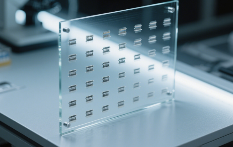
The glass substrate micro via refers to the through hole structure with small diameter and deep depth prepared on the glass substrate by micro processing technology. These vias usually have the characteristics of high precision and high consistency, which can meet the requirements of high-density integrated circuits and other miniaturized devices. The machining process of micro through-hole is usually realized by laser drilling, electroforming technology or mechanical drilling.
- Processing method:
- Laser processing: The laser processing technology makes the glass substrate locally heated and evaporated through the high energy density of the laser beam to form micro via. This method can accurately punch holes on glass materials with high hardness, and the pore size can reach the nanometer level.
- Electroforming technology: The metal template of micro via is formed on the glass substrate by electroforming technology, and the metal is deposited on the glass surface by electrochemical reaction, so as to manufacture the micro via with high precision.
- Mechanical drilling: The traditional mechanical drilling method is usually used for the glass substrate with large aperture, but with the improvement of drill bit precision, the application of this method in microporous manufacturing has also developed.
- Optical properties: Glass substrate has excellent optical performance, especially in the ultraviolet and visible light areas, so it is widely used in display screen, optical fiber communication and other applications. When machining micro via, the optical properties are closely related to the aperture, depth and wall quality, which determines its performance in optical devices.
2、 Technical challenges of glass substrate via
Although glass substrate micro via has broad application prospects in many fields, it still faces a series of technical challenges in the actual production process.
- Control of aperture and precision: The hardness and brittleness of glass substrates make pore size control a challenging task. Especially in the process of micro and nano aperture machining, any small error may affect the overall performance of devices. How to accurately control the hole diameter, hole depth and hole wall quality is a major problem in current technology.
- Hole wall quality: The wall quality of micro via directly affects its subsequent electrical performance, thermal conductivity, etc. The smoothness and crack free of the hole wall is the key to ensure that the through hole can play its function efficiently. In common processing methods, laser drilling can rapidly process high-precision micro via, but it is easy to cause thermal damage to the hole wall and affect the quality of the via.
- Material selection: There are many kinds of glass, including soda lime glass, aluminosilicate glass, etc. Different kinds of glass have different physical and chemical properties when machining micro through-hole. Therefore, when selecting glass substrates, comprehensive evaluation should be carried out according to specific applications. For example, in the field requiring higher optical performance, glass materials with lower refractive index should be selected, while in the field of electronic packaging, glass substrates with higher heat resistance and insulation performance should be selected.
- Cost control: The machining of micro through-hole involves many links, especially the manufacturing of high-precision micropores, which requires high processing equipment and material costs. This makes cost control in mass production an important consideration. How to improve the processing efficiency, reduce the cost, and at the same time ensure the accuracy of the hole diameter and the quality of the hole wall is a problem that must be solved in industrial applications.
3、 Engineering Application of Micro via on Glass Substrate
The glass substrate micro via technology has shown great application potential in many high-tech fields, especially in integrated circuit packaging, sensors, displays and other fields.
- Electronic packaging and integrated circuits: With the shrinking size of integrated circuits, packaging requirements are becoming increasingly complex. Micro via can realize electrical connection between different layers. Especially in 3D integrated circuit packaging technology, micro via is used to connect circuits between different layers. The glass substrate micro via can not only improve the density of the circuit, but also provide better thermal conductivity and stability, solving the thermal management problem in traditional packaging technology.
- Optical display and sensor: In the field of optical display, glass substrate micro via is widely used in the manufacturing of LED and LCD displays. Micro through-hole can help enhance light transmission, display effect and brightness. In addition, optical fiber sensors often need to use glass substrate micro via to achieve accurate optical signal transmission and acquisition.
- 3D printing and microfluidic chip: Micro via technology has been widely used in 3D printing and microfluidic chips. 3D printing technology can use glass substrates as support materials to build complex structures on a micro scale. Microfluidic chips transmit micro liquids through micro vias on glass substrates for biomedical, chemical analysis and other fields.
- Micro motor and sensor array: The glass substrate micro via technology is also used in the production of micro motors and sensor arrays. For example, in gas sensors or biosensors, micro via can be used to conduct gas or liquid to ensure high sensitivity and accuracy of sensors.
4、 Development trends and future prospects
With the continuous progress of manufacturing technology, the precision and reliability of glass substrate micro via will continue to improve. In the future, the glass substrate micro via technology may develop in the following directions:
- Nano hole processing: With the development of nanotechnology, the aperture of micro via is expected to be further reduced, even to the nanometer level, so as to meet the requirements of higher precision electronic and optical devices.
- Application of new materials: In addition to traditional glass materials, the application of new composite materials or metamaterials may lead to higher performance substrate materials, further improving the application range of micro via technology.
- Cost optimization and industrialization: With the optimization of production process and the continuous upgrading of equipment, the production cost of glass substrate micro via technology will gradually reduce, and it is expected to usher in a broader industrial application in the future.
5、 Conclusion
The glass substrate micro via technology has a broad application prospect in modern manufacturing industry. Its precision and stability make it an indispensable basic technology in many high-tech fields. With the continuous progress of manufacturing technology, micro via technology will play an increasingly important role in integrated circuit packaging, optical display, sensors and other fields. By overcoming the existing technical challenges, the glass substrate micro via will further promote the development of electronics, optics, medical and other industries.